What is a Diode and How it Works
What is a Diode
A diode is a p-n junction device that allows current to pass through it in only one direction, the forward direction.
A good example is a blocking diode found in charge controllers of solar systems. A blocking diode allows current to flow only from the solar panel to the battery.
The blocking diode prevents the movement of current from the battery back to solar panels when there is no sunlight.
Diode Symbol

Construction
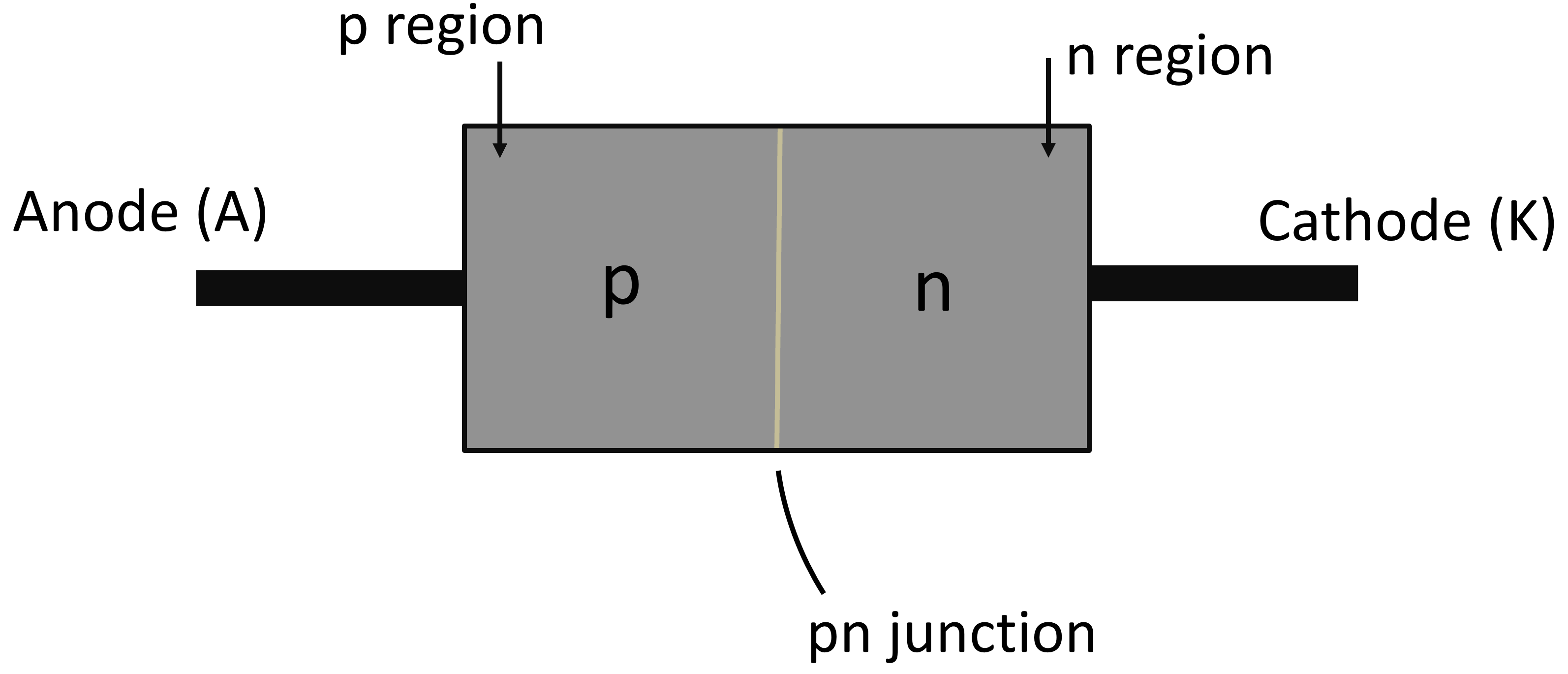
A diode in construction consists of two doped semiconductor materials joined together, namely the n-type material and the p-type material. The boundary separating the two materials is called the p-n junction.
Semiconductors are poor conductors of electricity at room temperature. Howeve,r they are doped (the addition of a controlled amount of impurities to semiconductor material) to improve their conductivity.
NB - The conduction of electricity in doped semiconductors is slightly different from that in conductors; that is why semiconductors are important in electronic engineering.
Silicon and germanium are the semiconductor materials commonly used in diodes.
A p-type material is a semiconductor material doped with atoms of group 3 such as boron (B). An n-type material is a semiconductor material doped with atoms of group 5 such as phosphorus (P).
How Doping Improves Conductivity in Semiconductor Materials
When a semiconductor material is doped with group 5 atoms, there is creation of free electrons (negative charges).
These free electrons will initiate conduction in the n-type material when connected to a source of voltage.
When a semiconductor material is doped with group 3 atoms, there is creation of holes (positive charges) that will cause conduction in the p-type material when connected to a source of voltage.
The Formation of the P-N Junction, Depletion Region and Barrier Potential
When the p-type and n-type materials are joined together, a p-n junction is formed. A p-n junction is a region separating the two joined materials.
As soon as the p-n junction is formed, certain activities take place near the junction resulting in the creation of two layers of opposite charges on the two sides of a p-n junction.
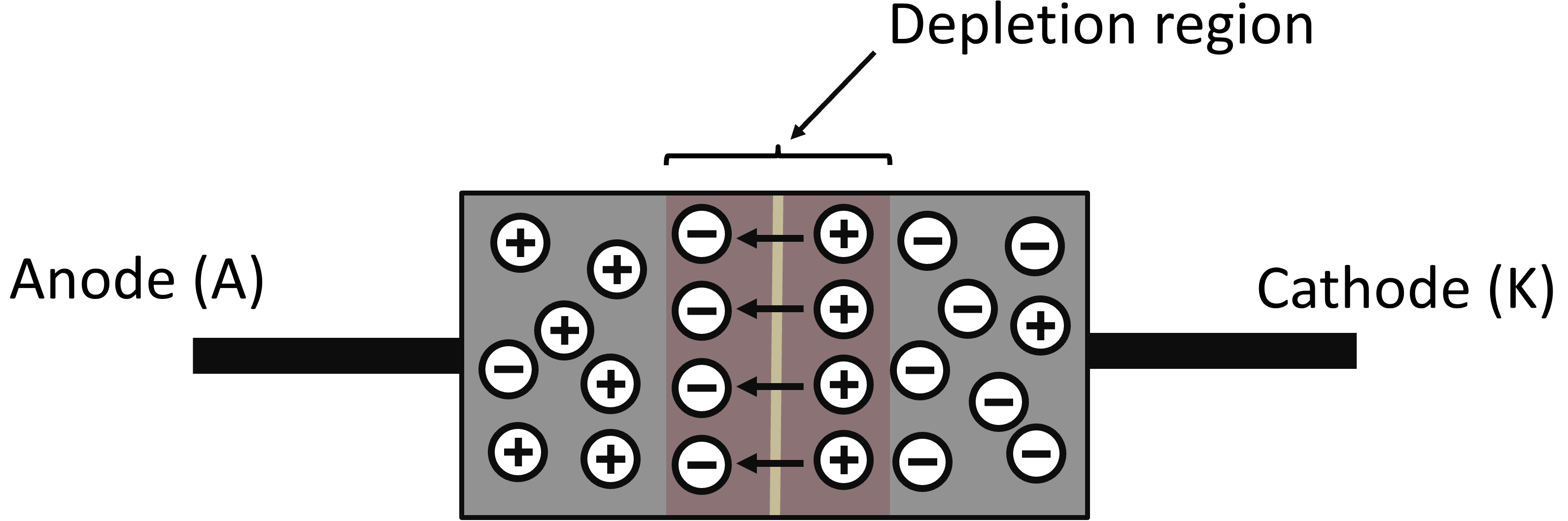
The two layers of opposite charges form a depletion region. The two layers of opposite charges also create an electric field that prevents further movement of electrons from crossing the junction.
The voltage of the electric field that prevents electrons from crossing the junction is called the depletion barrier potential.
In diodes made of silicon, the barrier potential is approximately 0.7V. In germanium diodes, the barrier potential is approximately 0.3V.
The barrier potential depends on the semiconductor material used, level of doping and temperature.
How a Diode Works
As mentioned earlier, a diode is a device that allows current to pass through it in only one direction.
To understand how a diode works and other electronic devices, we first need to look at electric current and electrons regarding their directions of flow.
The definition of current says, "current is the flow of electrons", but electrons flow from negative to positive while current is considered to flow from positive to negative.
The flow of current from positive to negative was due to the first discovery of electric fluid which was thought to be the cause of current before the discovery of electrons.
After the discovery of electrons, it was found that electrons are the ones that cause current, not electric fluid. However, the direction of current was not changed due to some reasons.
Let's look at what happens when a diode is connected in forward direction and in reverse direction. The process of applying a DC voltage source to a device (diode) to study how it works is called biasing.
Forward Biasing
Forward biasing is a condition that allows current through a diode.
To connect a diode in the forward direction, the p-type side of the diode is connected to the positive side of the battery and the n-type side is connected to the negative side of the battery.
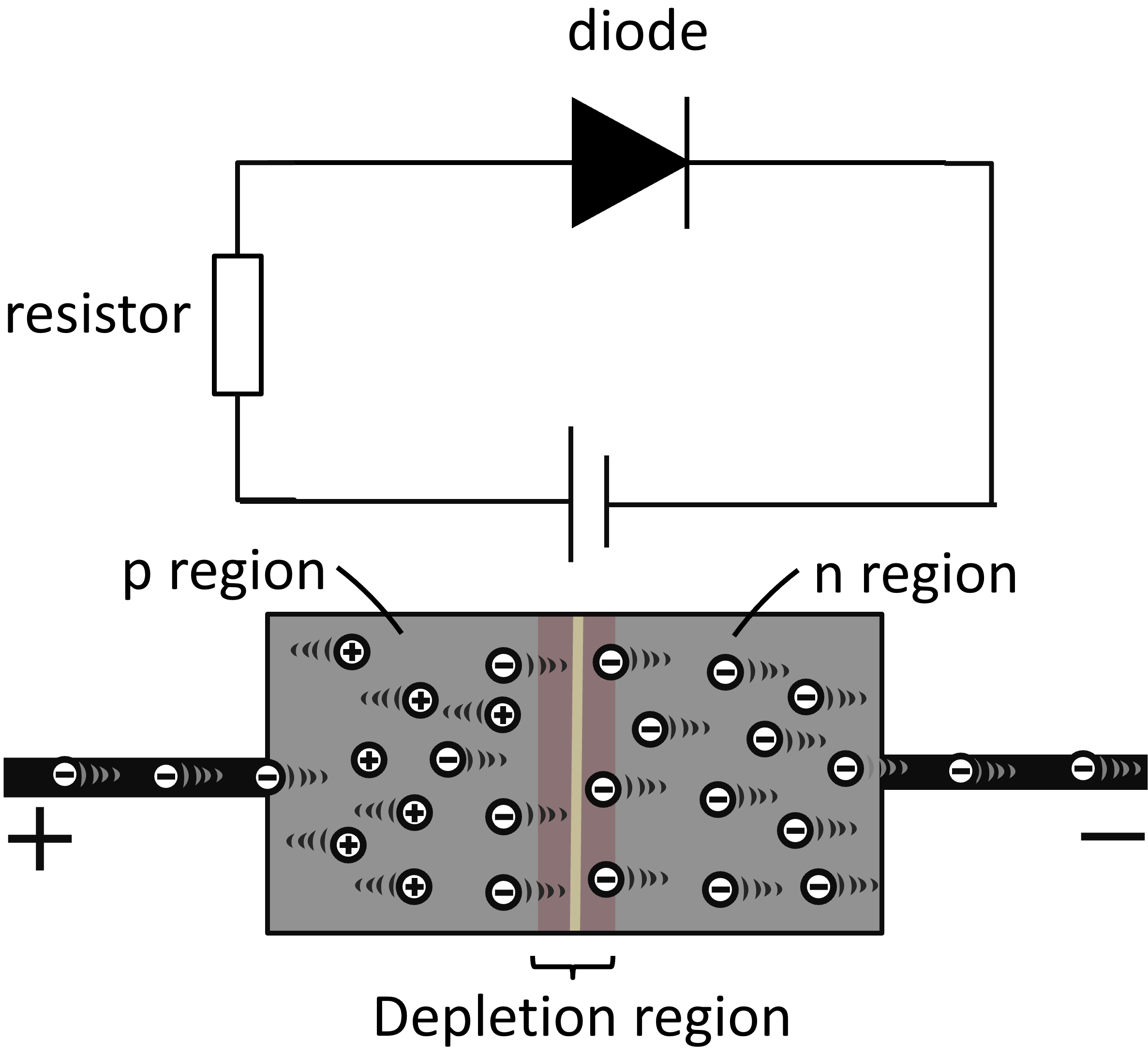
The resistor in the circuit limits current to a value that does not cause damage to the diode.
How current flows through a diode in forward direction
As the negative side of the battery is connected to the n-type side of the diode, it repels free electrons in the n-type side, pushing them towards the p-n junction.
The negative side also provides a continuous supply of electrons to the n-type side.
If these free electrons moving towards the p-n junction are given a force in the form of voltage usually equal to the barrier potential, they will use that energy to pass through the depletion region.
When electrons cross the depletion region, they combine with holes in the p-type region and start moving from hole to hole towards the positive side of the battery, as they are attracted by the positive side of the battery.
In this way, the diode allows current to flow in the forward direction.
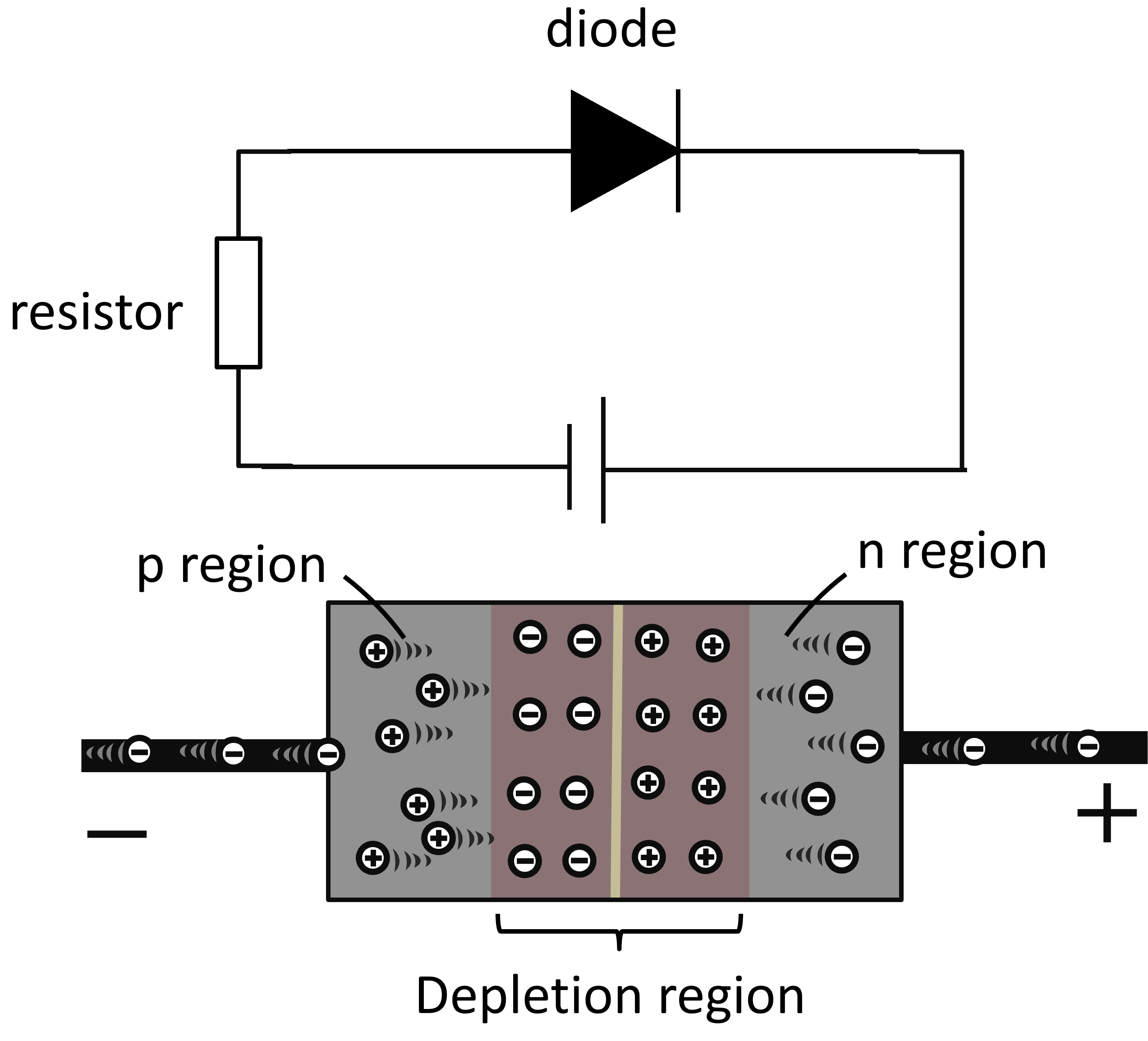
Reverse Biasing
Reverse biasing is a condition that does not allow current to flow through a diode.
To connect a diode in the reverse direction, the p-type side of the diode is connected to the negative side of a battery, and the n-type side is connected to the positive of the battery.
How current is blocked from flowing through a diode in the reverse direction
As the positive side of the battery is connected to the n-type region, it attracts free electrons from the n-type side away from the junction, creating more holes near the p-n junction in the n-type material
And at the same time, the negative side of the battery supplies free electrons to the p-type material, adding more electrons near the junction.
The addition of holes in the n-type material and electrons in the p-type material near the junction causes the widening of the depletion region, and the creation of an electric field with a voltage equal to the supply, resulting in no flow of current.
In reverse biasing, if the supply voltage is increased to the diode breakdown voltage, current will start to flow in reverse and the diode will be damaged.
Breakdown voltage (VBR) is the minimum voltage at which the p-n junction breaks down, resulting in a sudden rise in reverse current.
V-l Characteristic Curve
The results of connecting a diode in forward and reverse directions to a variable voltage supply can be plotted on a graph called the V-I characteristic curve.
The following diagram shows a V-I characteristic curve, the vertical axis shows current values and the horizontal axis shows voltage values.
NB - A variable voltage supply is a supply that allows us to adjust the voltage, enabling us to observe the diode's behavior at specific voltage values.
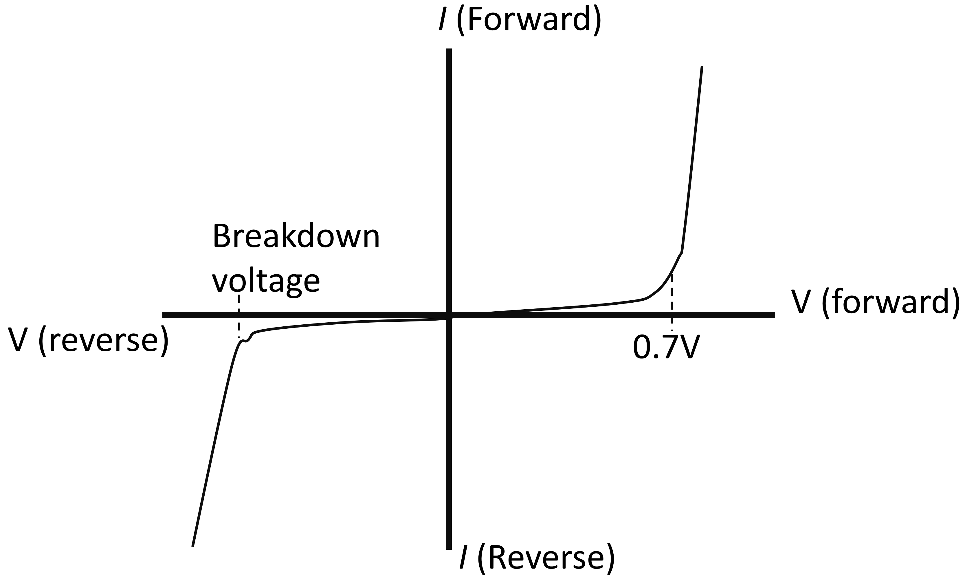
The left side of the vertical axis of the graph shows a diode connected in the reverse direction. The right side shows a diode connected in the forward direction.
V-I Characteristic Curve Explanation in the Context of a Complete Silicon Diode Model
NB: When explaining how a diode works, performing calculations, and troubleshooting a diode - determining whether a diode is functional or faulty, there are diode models that are used.
For example, our explanations in this article are based on the complete diode model. There are three diode models: the ideal model, the practical diode model and the complete diode model.
In the complete diode model, all the characteristics of a diode are taken into account. In other models, some characteristics are omitted.
The graph shows that:
In the forward direction, when the supply voltage is 0V, there is no forward current.
When the supply voltage is gradually increased, the current through the diode and the voltage across the diode (the voltage required to push current to flow through the diode) gradually increase.
This very small current flowing below the barrier potential of a diode is called leakage current, which is common in diodes since nothing is perfect.
When the supply voltage is increased such that the voltage across the diode is equal to the barrier potential (0.7V), the current through the diode increases rapidly.
When the supply voltage continues to be increased, current continues to increase rapidly but the voltage across the diode increases very slightly.
The slight increase in voltage above 0.7V is due to the resistance of the doped semiconductor materials, often referred to as dynamic resistance.
In reverse direction, when supply voltage is 0V, there is no reverse current. When the reverse voltage is gradually increased, there is only a small reverse leakage current and the voltage across the diode gradually increases.
When the supply voltage is increased such that the voltage across the diode is equal to the breakdown voltage, the current through the diode increases rapidly.
When the supply voltage is increased above the breakdown voltage, the current continues to increase rapidly but voltage increases very slightly.
Diodes other than Zener diodes are not designed to operate at or above the breakdown voltage; these diode have a large breakdown voltage of about 50V.