How the P-N Junction, Depletion Region and Barrier Potential are Formed
Let's start with the basics and for that we need to look at materials used in electronic engineering.
In electronic engineering, semiconductors such as silicon and germanium are the most commonly used materials.
At room temperature, semiconductors are poor conductors of electricity.
However, their conductivity can be improved by increasing their temperature, or more importantly through the process of doping, making them useful in electronic engineering.
When a semiconductor is made to conduct well through the process of doping, we call this type of conduction "extrinsic conduction".
Extrinsic conduction means that the conduction is not from the semiconductor material itself but is due to the process of doping.
If the temperature of a semiconductor is increased, the semiconductor conducts well. This conduction is from the semiconductor itself due to the temperature increase; we call it intrinsic conduction.
Some Basic Concepts we need to Understand:
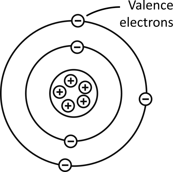
Materials such as conductors, insulators, semiconductors and more are made up of atoms. Atoms in turn are made up of electrons, protons, and neutrons.
Protons and neutrons are contained inside the nucleus of an atom. Electrons orbit around the nucleus of an atom in orbital shells.
Electrons in the outermost shell of an atom are called valence electrons. The outermost shell of an atom is called the valence shell. Valence electrons are the ones that take part in bonding and in conduction of electricity.
Electrons exist in either the valence band or the conduction band in a material. When electrons are in the valence band, they are not available for conduction. The electrons in the valence band are also called valence electrons.
When electrons are in the conduction band, they are available for conduction. Electrons in conduction band are called free electrons or conduction electrons.
In conductors, the valence band and the conduction band overlap, and electrons are always available for conduction.
In insulators, the gap between the conduction band and the valence band is very big, so electrons can't even jump from the valence band into the conduction band.
In semiconductors, the gap between the conduction band and the valence band is small. A small amount of energy is required for valence electrons to jump from the valence band into the conduction band.
How Increasing Temperature in Semiconductors Improve their Conductivity
A pure or intrinsic semiconductor is made up of atoms that have four valence electrons or four electrons in the outermost shell.
Since their outermost shell is not complete, each atom shares its outermost electrons with four nearby atoms in the material. The process of sharing outermost electrons by atoms is called covalent bonding.
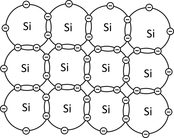
In covalent bonding, all valence electrons of each and every atom in a pure semiconductor material are involved, no electrons are left without forming a bond.
Since all valence electrons are involved in the process, there are no free electrons left, thus creating a chemically stable material. This material will not conduct at absolute zero temperature.
However, when the temperature of a semiconductor material is increased, valence electrons gain energy to break from covalent bonds and become free for conduction.
What is Doping
Doping is the process of adding a controlled amount of impurities to a semiconductor material to improve its conductivity.
Impurities added to semiconductor materials are elements from group 5 and group 3 in the periodic table.
Atoms of group 5 include phosphorus and arsenic. Atoms of group 3 include indium and boron.
If a semiconductor material is doped with atoms of group 3, the outcome is called a p-type material.
If a semiconductor material is doped with atoms of group 5, the outcome is called an n-type material. P-type and n-type materials are the basic building blocks for most electronic devices.
What Makes a Semiconductor Conduct Well After Doping
As mentioned earlier, semiconductor materials have four valence electrons while atoms of group 5 and group 3 have five and three valence electrons respectively.
When a semiconductor material is doped with atoms of group 5 such as phosphorus, there is always an electron from every phosphorus atom that is left without forming a bond.
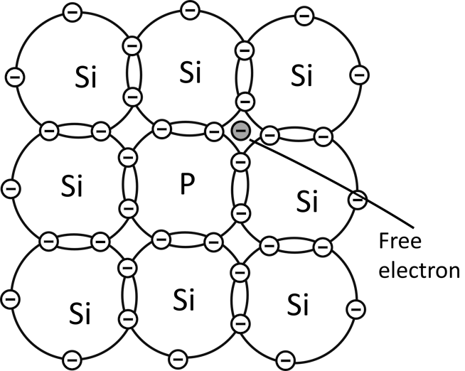
The phosphorus atom will share its four valence electrons with four silicon atoms surrounding it and left with an extra electron without forming a bond.
This electron from every phosphorus atom becomes free and initiates conduction when the material is connected to a voltage source.
Since conduction in the n-type material is initiated mostly by electrons, electrons are the majority charge carriers in the n-type material.
Holes also contribute to conduction in n-type material, but to a lesser extent. Holes are minority charge carriers in the n-type material.
When a semiconductor material is doped with atoms of group 3, such as boron, there is always a hole from every boron atom that is created in the material after covalent bonding.
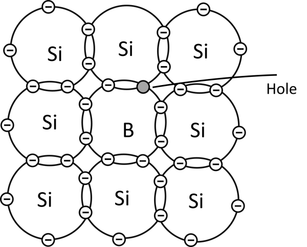
Boron atoms have three valence electrons while silicon atoms have four valence electrons.
After doping, all three valence electrons will be used, and since four are required to complete bonding with four silicon atoms surrounding it, a hole results from every boron atom.
This hole initiates conduction in the material when the material is connected to a voltage source.
Conduction in the p-type material is initiated mostly by holes; holes are the majority charge carriers.
Electrons also contribute to conduction in p-type material, but to a lesser extent; electrons are the minority charge carriers in the p-type material.
NB - In the n-type and p-type materials, free electrons and holes are created by the process of doping but the materials have an equal number of electrons and protons overal. The n-type and p-type materials are considered neutral.
When we take a piece of a p-type material and another piece of n-type material and join them together, a p-n junction is formed.
A P-N Junction
A p-n junction is a boundary that separates the joined p-type and n-type materials.
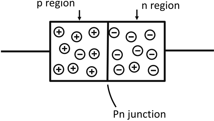
When p-type and n-type materials are joined together, there are several activities that take place near the junction that cause the creation of a depletion region.
Depletion Region
A depletion region is a region where the p-type and n-type materials are short or depleted of their majority charge carriers.
As soon as a junction is formed, randomly moving free electrons near the junction cross the junction to combine with holes in the p-type material.
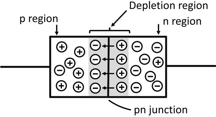
When electrons cross the junction, the n-type material loses electrons, causing a creation of a layer of holes (or a layer of positive charges) in the n-type material near the junction.
When electrons cross the junction to combine with holes in p-type material, they cause electrons to exceed holes in the p-type material. This results in the creation of a layer of excess electrons (or negative charges) in the p-type material near the junction.
The layer of excess electrons in the p-type material and holes in n-type material forms a depletion region.
In the depletion region, there are opposite charges on the sides of a p-n junction. Whenever opposite charges are near each other, there is a force acting between them. The force between the opposite charges forms an electric field.
As electrons cross the junction soon after formation of the p-n junction, the electric field will gradually increase in strength until it prevents the continual crossing of free electrons and the movement stops.
The voltage of the electric field is called the barrier potential. For electrons to cross the depletion region, they need a voltage that is equal to or above the barrier potential.
Barrier Potential
It is the amount of voltage required to move electrons across the depletion region.
The value of barrier potential depends on several factors that include the type of semiconductor material used, the amount of doping, and temperature.
The typical value of barrier potential for silicon is 0.7V and for germanium is 0.3V.
In the next articles you will see the p-n junction, depletion region and barrier potential in action.
The p-n junction is the basis for various electronic devices such as:
Transistors etc.,
which we looked separately in other articles.